Computer Architecture
Introduction
von Neumann architecture: shared memory banks + buses for instructions and data
Harvard architecture: seperate memory banks + buses for instructions and data
CPU-Memory Gap: increasing difference in speeds between DRAM, disk, and CPU speeds
- contributor to the Memory Wall: the point where a program’s speed is entirely determined by memory speed
Eight Great Ideas in Computer Architecture
- Use abstraction to simplify design
- Design for Moore’s Law
- Make the common case fast
- Performance via parallelism
- Performance via pipelining
- Make the common case fast
- Hierarchy of memories
- Dependability via redundancy
CPU
Runtime of a program determined by:
- CPU clock speed
- Type of instructions performed (e.g. multiplication/division take longer than addition/subtraction)
- Memory speed (access time)
Performance largely measured through throughput, latency, and clock speed.
CPI
CPI = clock cycles per instruction = average CPI = effective CPI
CPU time = CPI $\times$ instruction count $\times$ clock cycle
Power
power wall: limitation in processor development preventing processors from consuming any more power
- decreasing transistor size lowers voltage but increases power density, causing extra heat
- reducing voltage usage is hard, removing extra heat is even harder
- reason for possbile failing of Moore’s Law
- alternative: use multi-core processors or multiprocessors
Memory Hierarchy
The memory hierarchy was introduced to tackle the memory wall and reduce the effects of the Processor-Memory gap. Also:
- fast storage technologies (SRAM) are expensive and take more room
- gap between DRAM (main memory) and CPU continues to widen
- principle of locality
Principle of Locality
temporal locality: recently accessed items are likely to be accessed again in the near future
spatial locality: recently accessed items are likely to have nearby items accessed in the near future
Cache Hierarchy
CPU looks in L1 cache, then L2, then L3, then main memory.
NOTE: despite the numbering, L3 is a “lower level cache” than L2, which is a lower level cache than L1.
placement (mapping) policy: where should a new block to be loaded in the cache go? replacement policy: which block should be evicted from the cache (to load a new block)
cold miss (at level $k$): occurs when a block is missing for the first time at level $k$; these are unavoidable
conflict miss (at level $k$): mapping policies dictate where blocks can go in the cache: conflict misses occur when multiple data items from level $k + 1$ map to the same position in level $k$
capacity miss (at level $k$): a conflict miss that occurs because the cache is full: these would occur even if the cache was fully-associative with LRU replacement
Cache and Memory Performance
With caching, the CPU time formula changes:
CPU Time = instruction count $\times$ clock cycle $\times$ (CPI + average memory stall cycles)
Average memory stall cycles = access rate $\times$ miss rate $\times$ miss penalty
(CPI + average memory stall cycles) is called CPI stall CPI inside CPI stall is also called CPI ideal
banked cache: cache divided into two sections: one for instructions and one for data: L1 is usually banked cache
unified cache: cache where instructions and data are stored together
average memory access time (AMAT): average time to access memory considering both hits and misses
AMAT = hit time + miss penalty $\times$ miss rate
For multiple cache levels:
AMAT = L1 hit time + L1 miss rate $\times$ L1 miss penalty
L1 miss penalty = L2 hit time + L2 miss rate $\times$ L2 miss penalty
…
L3 miss penalty = Main memory hit time
Cache Implementation
Hierarchy management:
- registers <-> cache memory: compiler decides which values goes into registers
- cache memory <-> main memory: cache controller (hardware) handles memory movement
- main memory <-> disk: OS (virtualization), TLB (hardware), programmer (files)
The cache is split into $S$ sets, with $B$ blocks in each. Each block has a tag field used to differentiate between different items currently loaded in the cache.
A memory address is decomposed as the tag | set index | block offset
Addresses are assumed to be byte addresses (not word addresses).
Cache Organization Schemes
direct-mapped: one block per set; each memory address mapped to exactly one line in the cache; no tag needed
fully associative: one set: memory address can be mapped to any block; tag is whole address except block offset
N-way set associative: N sets
Set Associativity Cost
- N comparators for LRU, MUX delay, can’t assume a hit and recover later (since block isn’t available until after hit/miss decision)
Handling Cache Hits and Misses
Read hit: do nothing
Write hit policies (data only)
- write-through: maintain consistency between cache and main memory by writing to cache AND main memory; amortize performance by using a write buffer
- write-back: allow inconsistency, marking blocks as dirty when written to. Only write back to main memory on eviction (requires >2 cycles, 1 to check dirty and 1 to write-back; alternatively, use write-buffer for just 1 cycle)
Read miss policies:
- stall execution, fetch block from lower cache level, install into higher cache level, and resume
Write miss policies (data only): stall execution and
- write-allocate: fetch block from lower cache, write updated value, and install in cache
- no write-allocate: write to lower cache without installing into cache (or use a write buffer)
Cache Design
- primary cache should focus on minimizing hit time
- secondary caches should focus on minimizing miss penalty of primary cache
Reducing hit time:
- smaller cache size, smaller block size
- direct-mapping
- use write buffer for write-through/write-back policies
Reducing miss rate:
- larger cache, larger block size
- increase associativity
- use victim-cache: cache of most recently evicted blocks
Reducing miss penalty:
- smaller block size
- use write-buffer
- check write-buffer/victim cache on read miss
- use multi-level cache
- faster main memory
- improve memory bandwidth for memroy transfer between cache levels
Boolean Algebra
conjunctive normal form (CNF): conjuction of disjunctions
disjunctive normal form (DNF): disjunction of conjunctions
A set of operators is functionally complete if it is enough to describe any operation in boolean algebra
- NAND, NOR, $\lbrace \land, \neg \rbrace$, $\lbrace \lor, \neg \rbrace$ are functionally complete
Stateless Circuits
combinational circuits = stateless circuits = functional blocks
- circuits whose output depend solely on its inputs
block (schematic) diagram: specifies inputs, outputs, number of bits for each, and formula/truth table
1-bit half-adder: XOR gate for sum, AND for carry
1-bit full-adder:
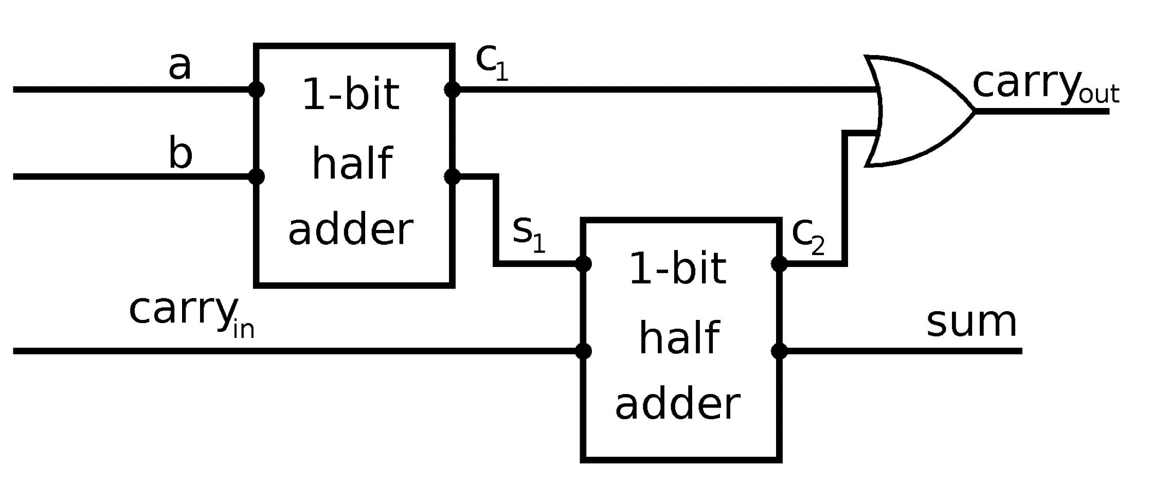
n-bit full-adder:
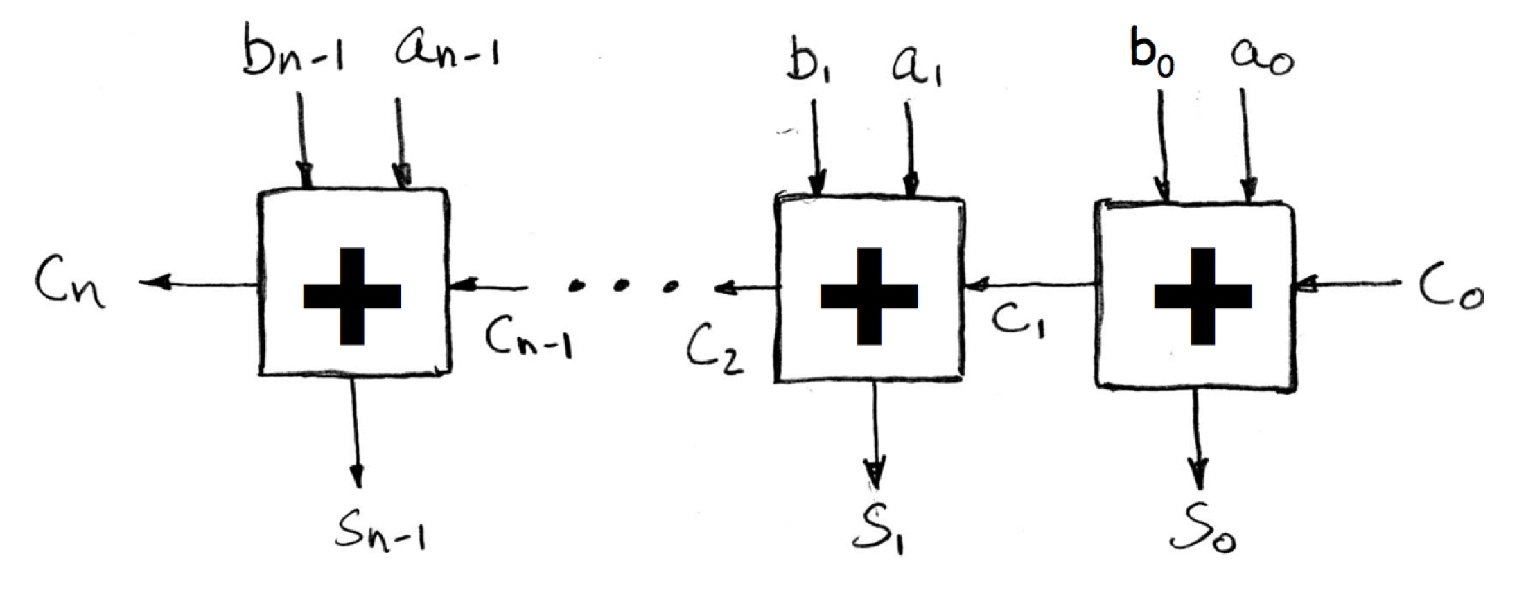
- unsigned addition: overflow if last carry bit $c_n$ is 1
- signed addition: overflow if $c_n \oplus c_{n - 1}$
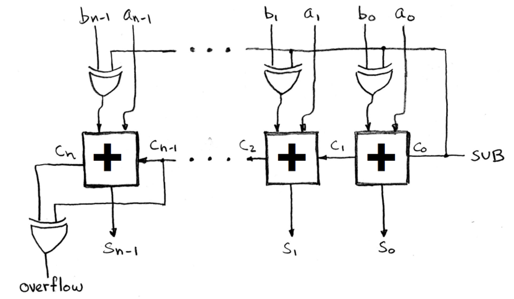
n-bit subtractor:
multiplexer: select between multiple inputs with control signal $c$:
\[MUX(a, b, c) = a \bar c + b c\]- output $a$ when $c = 0$ and $b$ when $c = 1$
demultiplxer chooses among its outputs
State Circuits
- combinational circuits cause propagation delay: need to synchronize with a clock
- faster components use a clock multiplier
delay flip-flop: sets state to input after some delay
| $D$ | $Q$ | $Q_{next}$ |
|---|---|---|
| 0 | 0 | |
| 1 | 1 |
toggle flip-flop: $T$ toggles state if $T \equiv 1$, otherwise does nothing
SR flip-flop:
- $S \equiv 1$ sets the state
- $R \equiv 1$ clears the state
- $S \equiv 0, R \equiv 0$ doesn’t change anything
- $S \equiv 1, R \equiv 1$ not allowed
JK flip-flop: SR flip-flop except both set to 1 toggles the state
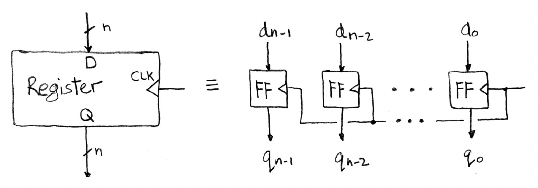
parallel-in parallel-out:
serial-in parallel-out:
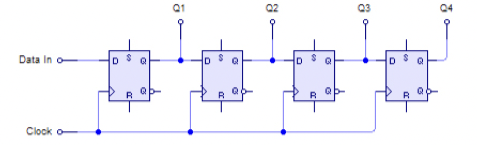
serial-in serial-out: one input bit, one output bit
parallel-in serial-out: one bit output at a time, bits shifted over on each output; requires additional control signal for write/shift operation
clk-to-q delay: propagation delay of a flip-flop
setup time: stable signal value to the input of a flip-flop required before the rising edge of the clock
hold time: stable signal value to the input of a flip-flop required after the rising edge of the clock
- usually less than clk-to-q delay
clocked accumulator:
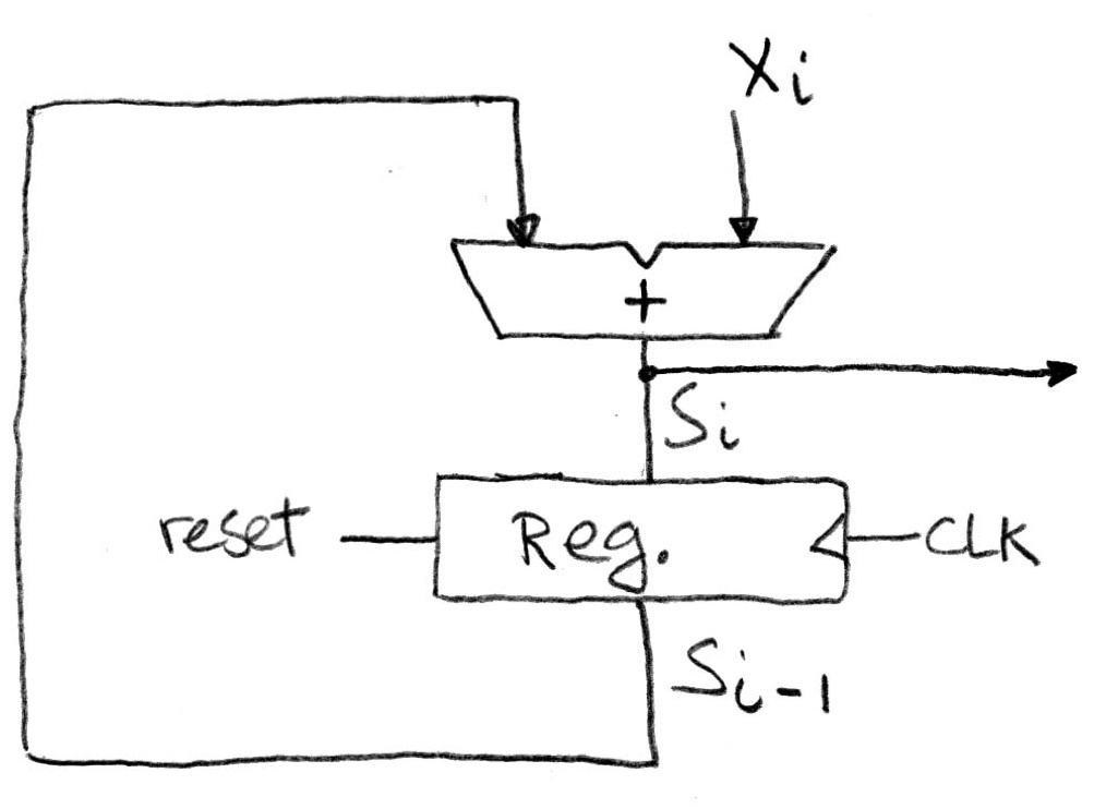
- note that we only need to clock the register, not the combinational circuit
minimum clock period = combinational circuit delay + clk-to-q delay + setup time
Finite State Machines
Mealy machine: FSM whose output depends on current state and current input
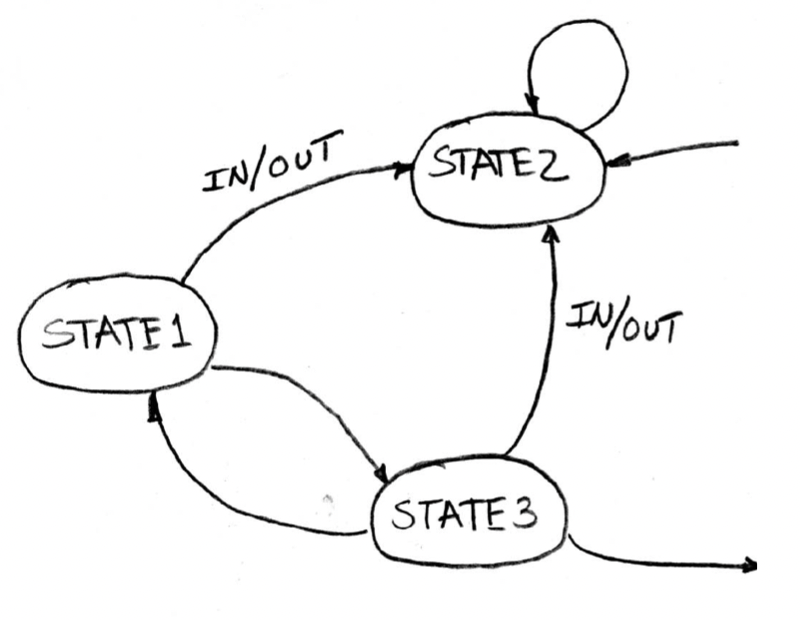
- Generate truth table
- Simplify boolean expressions for next state and output bits
- Draw logic diagram
Introduction to MIPS
MIPS ISA is a RISC architecture with pipelining and without interlocking.
MIPS is big-endian.
MIPS Registers
32 32-bit registers
- $0 always holds the value 0
- $at reserved for compiler
- $v0-v1 return values
- $a0-a3 arguments
- $t0-t9 temporaries
- $s0-s7 saved registers (must be saved/restored by the callee)
- $gp global pointer for static data
- $fp frame pointer
- $sp stack pointer
- $ra return address
MIPS Instruction Formats
R-type (register) instructions
| opcode | source 1 | source 2 | destination | shift amount | function type |
|---|---|---|---|---|---|
| 6 bits | 5 bits | 5 bits | 5 bits | 5 bits | 6 bits |
- for instructions that use
shamt(shift amount), source 1 is always 0- e.g.
sll $s0, $t0, 4- source 1 = 0
- source 2 =
$t0 - destination =
$s0 - shamt = 4
- e.g.
- for arithmetic instructions, function type determines the function the ALU will perform (opcode is usually 0 here)
I-type (immediate) instructions
| opcode | source 1 | source 2 (or destination) | immediate |
|---|---|---|---|
| 6 bits | 5 bits | 5 bits | 16 bits |
- note for
sw $t1, 32($t0),$t1is the destination and$t0is the source - relative PC addressing: branch immediates are multiplied by 4 before being added to the PC
J-type (jump) instructions
| opcode | target (jump address) |
|---|---|
| 6 bits | 26 bits |
- only
jandjalinstructions - pseudo-direct addressing:
targetis multiplied by 4 and OR-ed with the upper 4-bits of the PC to form the new PC
MIPS Single-Cycle Datapath
minimum clock cycle needs to be long enough to run all 5 stages in one clock cycle
Instruction Fetch
- Update value of PC on rising clock edge
- Fetch instruction from memory and pass to next stage
- Compute PC + 4
Instruction Decode
- Decompose instruction into bit segments
- Read opcode, determine R/I/J instruction type
- Access operand values from registers
- Extend to 32-bit immediate if needed
Execute
- do the actual work of the instruction in the ALU: add, subtract, shift, etc.
- for data-transfer instructions, compute the absolute address from the immediate and base address
Memory Access
- access memory with the address calculated in the execute stage
Write Back
- write back the calculated/accessed value to the destination register
Multiplexers needed in datapath for:
- choosing between PC + 4 and PC branch/jump
- write-back from ALU or from memory
- choosing between register or immediate for ALU input